Experienced Manufacturers
Production plant area of more than 10,000 square feet, more than 100 people construction team.
 Hotline
Industry Introduction
Semiconductors are mainly used in integrated circuits, consumer electronics, communication systems, photovoltaic power generation, lighting, high-power power conversion and other fields, whether from the point of view of science and technology or economic development, the importance of semiconductors is very great. Common semiconductor materials include silicon, germanium, gallium arsenide, etc. Silicon is one of the most influential of the various semiconductor material applications. Semiconductor refers to the material whose conductivity at room temperature is between a conductor and an insulator. Most of the electronic products, such as computers, mobile phones or digital recorders in the core unit and the semiconductor has a very close relationship.
Pollution hazards
The production process of semiconductor materials will produce volatile organic compounds and dust, organic emissions are mainly generated in the sub-assembly line, the emissions generated depend on the different components, such as: hexachloroethylsilane loading line, (diethylamine) silane sub-assembly line, tetramethylsilane sub-assembly line, hexamethyldisiloxane sub-assembly line, etc., and volatilisation in the electric heating and drying.
Overview of Semiconductor Exhaust Treatment Programme
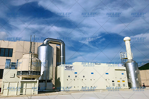
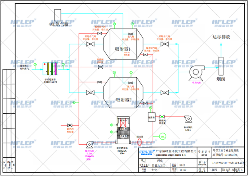
For the semiconductor exhaust VOCs treatment technology, now in line with environmental emission requirements, and play a cost-effective treatment technology, is the use of reduced wind concentration + combustion method of treatment technology is more economical and energy-saving. It is recommended to use: wet jet washing (multi-pipe) + dry filter + reduced wind enrichment + catalytic combustion combination of governance, governance can meet the emission requirements of standards!
Process flow
Wet jet washing (multi-tube) + dry filtration + activated carbon adsorption and concentration + catalytic combustion process (integrated system) process treatment. Organic waste gas is collected through pipeline, and enters into pretreatment wet jet tower to remove paint dew, acidity and particles of purification. After purification, the gas is introduced into the dry filter to remove particles and harmful substances on the activated carbon adsorption, and the organic waste gas is then sent to the activated carbon adsorption bed device, and the VOCs components in the waste gas are absorbed by the activated carbon and then discharged to the atmosphere in compliance with the standards. When the activated carbon adsorption bed is saturated by electric heating high temperature (80-100 ℃ C) desorption of VOCs substances, desorption of high concentrations of organic waste gas directly into the catalytic combustion co, through the accelerated oxidation of high concentrations of waste gas by precious metals, in ( 250-350 ℃) high temperature purification and oxidation of harmless carbon dioxide (CO2) and water vapour (H20) and meet the standards of emission into the atmosphere.
Other treatment technology solutions
Low concentration and small air volume semiconductor waste gas can be used: spray tower, uv photolysis purifier, activated carbon adsorption and other single or multiple combinations of processes for treatment;
High concentration of small air volume semiconductor waste gas can be used: pretreatment + zeolite molecular sieve + catalytic combustion, pretreatment + zeolite molecular sieve + RTO thermal storage incinerator, a single catalytic combustion device or a single RTO thermal storage incinerator and so on;
High concentration and large air volume semiconductor waste gas can be used: pretreatment + zeolite rotor concentration + catalytic combustion or pretreatment + zeolite rotor concentration + RTO thermal storage incinerator and so on.
Reason for choice

Production plant area of more than 10,000 square feet, more than 100 people construction team.

A number of engineers and technicians, most of whom have more than 10 years of experience and have worked on numerous projects.

Adoption of the latest domestic and international treatment technology, with high treatment efficiency.

According to the actual needs of the project, free to customise the corresponding exhaust gas treatment solutions, all regions of the country package to meet the emission standards.

Passed the third level of construction enterprise qualification and a number of technical patents...

1000+ project experience, more than 100 industry partners, complete environmental protection qualification.
Contact - Ways
Contact information
Catalytic combustion machine is a dry filter + adsorption de...

Activated carbon adsorption and desorption + CO catalytic co...

Zeolite rotor concentration + RTO regenerative incinerator c...

Zeolite rotor concentration + CO catalytic combustion proces...

CO catalytic combustion + TO direct combustion furnace proce...

For low concentration and low air volume of waste gas treatm...

0769-22277627 86159 1875 6640
service@hengfenglan.com
No.28, Yuanzhou Industrial Road, Shangjia, Wanjiang Street, Dongguan City, Guangdong Province, China
 Guangdong Public Security Bureau No. 44190002006305
Industry Introduction
Semiconductors are mainly used in integrated circuits, consumer electronics, communication systems, photovoltaic power generation, lighting, high-power power conversion and other fields, whether from the point of view of science and technology or economic development, the importance of semiconductors is very great. Common semiconductor materials include silicon, germanium, gallium arsenide, etc. Silicon is one of the most influential of the various semiconductor material applications. Semiconductor refers to the material whose conductivity at room temperature is between a conductor and an insulator. Most of the electronic products, such as computers, mobile phones or digital recorders in the core unit and the semiconductor has a very close relationship.
Pollution hazards
The production process of semiconductor materials will produce volatile organic compounds and dust, organic emissions are mainly generated in the sub-assembly line, the emissions generated depend on the different components, such as: hexachloroethylsilane loading line, (diethylamine) silane sub-assembly line, tetramethylsilane sub-assembly line, hexamethyldisiloxane sub-assembly line, etc., and volatilisation in the electric heating and drying.
Overview of Semiconductor Exhaust Treatment Programme
For the semiconductor exhaust VOCs treatment technology, now in line with environmental emission requirements, and play a cost-effective treatment technology, is the use of reduced wind concentration + combustion method of treatment technology is more economical and energy-saving. It is recommended to use: wet jet washing (multi-pipe) + dry filter + reduced wind enrichment + catalytic combustion combination of governance, governance can meet the emission requirements of standards!
Process flow
Wet jet washing (multi-tube) + dry filtration + activated carbon adsorption and concentration + catalytic combustion process (integrated system) process treatment. Organic waste gas is collected through pipeline, and enters into pretreatment wet jet tower to remove paint dew, acidity and particles of purification. After purification, the gas is introduced into the dry filter to remove particles and harmful substances on the activated carbon adsorption, and the organic waste gas is then sent to the activated carbon adsorption bed device, and the VOCs components in the waste gas are absorbed by the activated carbon and then discharged to the atmosphere in compliance with the standards. When the activated carbon adsorption bed is saturated by electric heating high temperature (80-100 ℃ C) desorption of VOCs substances, desorption of high concentrations of organic waste gas directly into the catalytic combustion co, through the accelerated oxidation of high concentrations of waste gas by precious metals, in ( 250-350 ℃) high temperature purification and oxidation of harmless carbon dioxide (CO2) and water vapour (H20) and meet the standards of emission into the atmosphere.
Other treatment technology solutions
Low concentration and small air volume semiconductor waste gas can be used: spray tower, uv photolysis purifier, activated carbon adsorption and other single or multiple combinations of processes for treatment;
High concentration of small air volume semiconductor waste gas can be used: pretreatment + zeolite molecular sieve + catalytic combustion, pretreatment + zeolite molecular sieve + RTO thermal storage incinerator, a single catalytic combustion device or a single RTO thermal storage incinerator and so on;
High concentration and large air volume semiconductor waste gas can be used: pretreatment + zeolite rotor concentration + catalytic combustion or pretreatment + zeolite rotor concentration + RTO thermal storage incinerator and so on.

 >
>